Obsolescence Guaranteed
Recommended: Gigatron
a computer w/o a microprocessor
The 6X0X Boards
Adding N8VEM ECB cards to create a fully independent 6X0X system, source: here
Background
6800-family CPUs were first brought on the N8VEM platform through a 6809 prototype board developed by Andrew Lynch. The board saw a lot of ‘evolution’ going from early prototype to its current, second version. Next to the 6809, it can host 6502 or 6802 CPUs. Through the work of Dan Werner, each CPU is now provided with its own operating system and ROM monitor.
Next to the SBC board, two optional expansion boards were developed: the Mezzanine IO board and the ECB Bridge board. The first adds I/O to the Processor board, the latter is a backplane that allows normal ECB peripheral cards to be added. This opened up the choice to run the 6x0x SBC in two different modes:
- Hosted mode. The 6x0x Processor board is a peripheral in the Z80 N8VEM system. On-board, the 6x0x lives its own life with its own operating system, but a CP/M server program delivers console and disk I/O. The Mezzanine board can be used to add more I/O to this setup.
- Stand Alone mode. Coupled to the 6x0x mezzanine board, the 6x0x processor board can also run on its own. The Bridge board allows this system to use existing ECB peripherals, like the VDU or Disk IO boards.
All of this means there are multiple ways to operate the 6x0x boards, with multiple CPUs and operating systems. That flexibility is impressive, but also makes it easy to lose oversight. You can just use the Processor board in a Z80 N8VEM system, or end up with a stand-alone machine as shown in the two pictures below.

The 3 6x0x boards stacked, source: here

Background
6800-family CPUs were first brought on the N8VEM platform through a 6809 prototype board developed by Andrew Lynch. The board saw a lot of ‘evolution’ going from early prototype to its current, second version. Next to the 6809, it can host 6502 or 6802 CPUs. Through the work of Dan Werner, each CPU is now provided with its own operating system and ROM monitor.
Next to the SBC board, two optional expansion boards were developed: the Mezzanine IO board and the ECB Bridge board. The first adds I/O to the Processor board, the latter is a backplane that allows normal ECB peripheral cards to be added. This opened up the choice to run the 6x0x SBC in two different modes:
- Hosted mode. The 6x0x Processor board is a peripheral in the Z80 N8VEM system. On-board, the 6x0x lives its own life with its own operating system, but a CP/M server program delivers console and disk I/O. The Mezzanine board can be used to add more I/O to this setup.
- Stand Alone mode. Coupled to the 6x0x mezzanine board, the 6x0x processor board can also run on its own. The Bridge board allows this system to use existing ECB peripherals, like the VDU or Disk IO boards.
All of this means there are multiple ways to operate the 6x0x boards, with multiple CPUs and operating systems. That flexibility is impressive, but also makes it easy to lose oversight. You can just use the Processor board in a Z80 N8VEM system, or end up with a stand-alone machine as shown in the two pictures below.

The 3 boards + ECB expansion cards + drives
The 3 boards as a stand-alone system
These three boards deserve a lot more attention from vintage computer enthusiasts that want to broaden out their horizons beyond CP/M. This text is the byproduct of building my own board set. It may be useful as a technical introduction; but because it is simply a bundling of my personal notes please do not take it as an authoritative or even competent guide to the boards.

1. The 6x0x Processor board
This is the main board, and actually the only one you need for running a full 6502 or 6809 system. Two versions exist:
Rev. 1: one socket for a 6809 CPU, but a 6502 can be used with a home-made socket adapter
Rev. 2: has dual 68xx and 6502 sockets
Description of the Rev.1 board:
This is a self-contained 1- or 2 Mhz 6809 SBC computer system with its own memory. A 28c16 (or 2716) ROM provides the 2k bootstrap, and a 628128 SRAM provides 60k of accessible RAM. A 6821 PIA is the single peripheral of the SBC and it does only one thing: talk to the on-board 8255. That 8255 is instrumental: it makes the whole stand-alone, independently operating SBC appear as a peripheral on the ECB bus. The Z80 N8VEM can then serve the 6809 card by providing the user console, (hard) disk services, and whatever else you may think of, all served to the 6809 through the parallel port of the 8255/6821 combo.
As opposed to the Z80, IO in the 6x0x world I/O is memory mapped. The SBC uses $0000-$EFFF for SRAM, $F000-F7FF as the IO region, and $F800-FFFF as the ROM region. That leaves 60K for RAM and only uses 2K each for IO and ROM spaces.
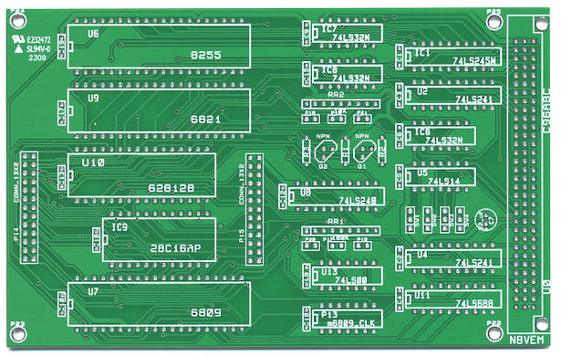
The Rev.1 board, with a single CPU socket. Source: here)
Jumpers and Settings:
Jumpers P16-P20 are normally on, but removing them allows users to interfere in the default chip select logic. Jumper P21 connects the 8255 interrupt signal to the ECB bus [why should it not be on – but DW states he leaves the jumper off?].
- P16 – connects the /CS_PIA to the 688 comparator. [why would you not want to do this?]
-
P17 – pulls mA16 to GND, getting rid of the upper 64k of the SRAM chip.
Remove jumper only if the mezzanine board is set up to control A16.
Remove jumpers P18,19,20 only when you want the Mezzanine board to intercept chip select signals. Rewiring them becomes necessary when operating the bus expansion port on the Mezzanine board (and consequently, the Bridge board), but not for anything else:
- P18 – connects /CS_ROM to the default chip select circuitry.
- P19 – connects the generic /CS_IO signal to the default chip select circuitry.
- P20 - connects /CS_RAM to the default chip select circuitry.
- P21- a jumper connects the ECB bus interrupt to the 8255’s INTR_A and INTR_B outputs.
Switches:
Four switches set the base address of the Processor board (to be precise, its 8255) as a peripheral on the ECB bus. SW1 sets address value of A7 to 0 or 1, SW2 covers A6, SW3 covers A5, SW4 covers A4. A3 and A2 are hard-wired to be 0 for the board address. See the appendix for default settings with various operating systems.
Lastly, two 26-pin headers rise up to provide access for the optional IO Mezzanine expansion board. P14 brings out the address and data lines (plus VCC and GND). P15 brings out the other lines.
Patches (correcting the RESET signal):
The Rev. 1 board gives a /RESET signal (active low) to the 8255, which in fact needs an active high RESET signal. Cut the input to 8255 U6 pin 35 and connect it to pin U5 pin 10. Without this, you will not be able to communicate with the 6809 host processor via the ECB.
Accommodating a 6502 CPU:
Rev. I of the Processor board has no separate socket for the 6502. Instead, a simple adapter socket can make a 6502 fit in the 6809’s socket.
1a. The Rev. 2 board and its changes
This board ‘s major improvement is a separate socket for a 6502. There’s no longer a need to have a home-made adapter socket to wedge a 6502 into the 6809’s socket.
Jumpers P16-P21 are as described for Rev.1. The old address select switches are now replaced by P26, which allows you to set A7 (jumper p1-2), A6 (3-4), A5 (5-6), A4 (7-8), A3 (9-10) and A2 (11-12).
New jumpers for Rev.2 boards:
- K1 – jumpering 2-3 gets the R/W signal from the 6809 socket, 1-2 gets it from the 6502 socket
- K2 – jumpering 2-3 gets the E signal from the 6809 socket, 1-2 gets it from the 6502 socket
- K3 – there is no K3, actually.
- K4 – off for 6809 (use its E), jumper 1-2 let 6502’s Phi2 (pin 39) drive E. Jumper 2-3 for 6802
-
K5 – off for 6809, jumper 2-3 to let CLK drive 6502’s clock input (pin 37),
jumper 1-2 for 6802 (the 6802 uses this pin for its clock output) -
JP1 – Leave off for 6809 operation. Put on for 6502 and 6802 operation.
Jumpering pulls 6809’s pin 35 (Q) to GND. - JP2 – Leave off for normal 6502 & 6809 operation. Jumpering pulls 6802 pin 35 (6802 VCC Standby, but NC on 6502) to GND. I do not understand the purpose behind the schematic – pin 35 is pulled high without JP2, but jumpering this brings a pull-down into play. Why would you connect pin 35 in-between? Are you supposed to cut the VCC trace for a 6802?
- JP3 – Leave off for normal 6502 & 6809 operation, but used for 6802. Jumpering connects 6802 pin 36 (RE but NC on 6502) to NC_A24 on the ECB bus. apparently this is to let a 6802 retain its 32 bytes of built-in memory, but AFAIK A24 is well and truly Not Connected. So why would a 6802 CPU benefit from this? More importantly, should it not be pulled to GND by default for 6802s?
-
JP4 – Leave off for normal 6502 & 6809 operation, but used for 6802.
Jumpering connects 6802’s pin 3 (MR) to the board’s MRDY signal.
Obtaining components:
Most ICs are available from the usual sources like Mouser or Jameco. The 6821 and 6809 are no longer carried by them, but eBay vendors offer them continuously.
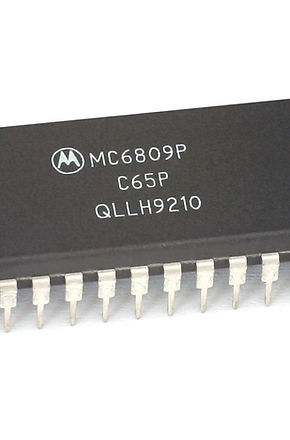
• 6809: Any version of the CPU will suit the board, but 1 Mhz parts (the 6809P is the most common)
will certainly not work with on 2Mhz – match the parts. For the 6821, the same is true.
• The 28C16 EEPROM is also no longer easily available. However, a 2716 can also be used.
Using a 6502 should also be reasonably uncomplicated. It should be kept in mind that running the system in Stand Alone mode requires a 2 Mhz 6502 for the Disk I/O board to run reliably. In Hosted Mode, of course, that is not relevant. New production runs of the 65C02, such as the one offered here by Mouser, should also be fine.

2. IO Mezzanine Board
This board adds I/O and allows the 6809 host processor to act as a stand-alone computer system, away from the Z80/ECB environment, if desired. It adds the following components:
• A 9V DC power connector (regulated down to 5V using a 7805)
• 6551 ACIA serial
• 6840 PTM programmable counter/timer
• Two 6522 VIA parallel IO with timers
• Expansion bus for future expansion
• Reset button
Although the above additions provided by the Mezzanine board make it possible for the 6809 to run as a stand-alone computer, the Mezzanine board can also be used in the Hosted mode (ie, using the Z80 N8VEM). In the Hosted Mode, it simply adds extra contacts to the outside world for the 6809.
Description:
• P7 and P8 are the connection to the CPU board (so solder on the reverse side of the PCB…)
• P9 is the serial port, RS-232 level with RTS/CTS as hardware handshaking possibility.
• P10 is the parallel port connector, bringing out 3 8-bit ports.
• P11 offers the other (control) pins from the 6522s
• P12 and P13 are the expansion bus interface, data and address buses are buffered by 244/245s but not all control signals are buffered.
The configuration latch:
This is the one important element of the Mezzanine board to understand. Only 3 of the 4 parallel ports are brought out for general use. The 4th port (PD0-7) is used internally as a configuration latch.
a. PD0 is connected to the ECB bus interrupt line, so the 6809 CPU can now interrupt the Z80 on
the SBC whenever it wants. PD0 should default to LOW so that the 74LS06 pulls the ECB bus
interrupt signal HIGH.
(Andrew Lynch:) When running the 6809 host processor with the IO mezzanine attached I recommend the Z80 CPU have code to handle a regular /INT interrupt. If the PD0 pull down resistor is not enough to pull the pin down and if the PD0 initializes as an OUTPUT set to HIGH, it will pull the Z80 CPU /INT line LOW until the 6809 configures the U7 PD0 to go LOW and release the Z80 from its interrupt.
b. PD1 disables ROM, allowing for future expansion cards on the 6x0x bus to use its address space
on demand. If this feature is to be used (no ROM expansion boards exist though) then use JP1
and JP2 as described further below.
PD1 should default to LOW so that the normal 6809 host processor ROM chip select works.
Setting it to HIGH would block the 6809 host processor ROM from being selected creating an
internal memory hole ($F800-$FFFF).
c. PD2 is similar and it can map out the RAM to allow an alternative RAM on the expansion bus.
This would be useful for a MC6845 style shared memory CRTC circuit or RAM expansion. PD2
should default to LOW so that it the normal 6809 host processor RAM chip select works. Setting
it to HIGH would block the 6809 host processor RAM from being selected creating an internal
memory hole ($0000-$EFFF).
d. PD3 is connected to the 6809 host processor A16 line so it allows the 6809 to use the upper 64K
of the 128Kx8 SRAM. That should work without any special configuration. [Except that jumper
P17 should then absolutely be left open on the processor board?]
e. Pins PD4-PD7 are exported to the 6809 IO mezzanine expansion bus to help configure expansion
RAM, ROM, and/or IO in the future.
Jumpers and settings:
• K2 - jumper pins 1 and 2. This connects the 6840 Timer Output 1 to /NMI (through the U1 inverter).
But note the patch for a missing trace on /NMI below.
• JP1 – ROM Select override. Normally, leave this open.
But: connecting pin 2 to [P18, pin 2] enables the 6809 IO mezzanine to "intercept" the
ROM chip select signal and add conditions to it before it is passed to the ROM chip.
• JP2 – RAM Select override. Normally, leave this open.
But: connecting pin 2 to [P20, pin 2] enables interception of CS_RAM on the processor
board for the same purpose.
• If the RAM/ROM override feature described above is installed, then pin 1 of both JP1 and JP2 are 10K pull up resistors and should be connected to Pin 1 of P18 and P20 respectively.
(Andrew Lynch:) It is probably not necessary but since there are longer signal paths and a chance for unconnected inputs the pull up resistors will prevent U11 (74LS32) from oscillating.
• U11 – this 74LS32 should normally notbe fitted and remain an empty socket, unless RAM/ROM
overrides are implemented.
Using the expansion bus:
Although the expansion bus exports everything from the CPU bus, it will only allow any importing if and only if all the RAM/ROM/internal IO chip selects are inactive. That should prevent bus contention. Since the 6809 host processor CPU memory map is full except for a portion of the IO address range the PD1 and PD2 are needed to prevent the internal RAM/ROM from being selected so they do not conflict with the bus expansion memory. This is where the complexity around JP1 and JP2, described above, come into play. If you do not want to use the expansion bus, ignoring this topic (and ignoring JP1 and JP2) are fine.
Patches and fixes:
A few connection traces were left out of the PCB. Do check whether this still applies to your board, newer versions may exist that have this fixed on the board already:
• add jumper from pin 1 of K2 to pin 3 of U1 (/NMI missing trace)
• add jumper from pin4 of U1 to R14 resistor on the pin not connected to VCC (/NMI missing trace)
One other patch is also generally needed:
• add jumper from pin 1 to pin 9 on the 6551, forcing ‘Clear to Send’ at all times.
This eliminates problems with CTS when using the serial terminal.
It may also be good to replace the reset button by a jumper: if the Bridge Board is used, the reset button is impossible to access.
Lastly, on the Rev. 1 Processor board, disconnect pin 12 of U5 if using the Mezzanine’s reset button [Not necessary on the Rev. 2 board as it buffers the ECB /RESET signal?].
Obtaining the parts:
• 6551 and 6840 are available through eBay dealers and the like – but easy to obtain
• The 6522 is also available new from Mouser etc. Buy the ‘S’ (Standard CMOS) version.
Introducing the Mezzanine board to your system:
1. The first step is to perform the 8255 reset mod if you have a Rev. 1 Processor board.
2. Then, get the Host Processor running with the N8VEM without the IO board attached.
If you download the "Cubix For the N8VEM 032310.zip" file from the m6809 folder on the WIKI,
there is a PDF in that archive that will walk you through getting the board running and getting
CUBIX installed.
3. Once you have this working, add the Mezzanine board. The Drivers.ASM file in CUBIX can be
changed to use the serial port as the console rather than the ECB to Z80 interface by changing
this:
FCB 1 CONSOLE INPUT DEVICE
FCB 1 CONSOLE OUTPUT DEVICE
to this:
FCB 2 CONSOLE INPUT DEVICE
FCB 2 CONSOLE OUTPUT DEVICE
3. Bridge Board (ECB Backplane)
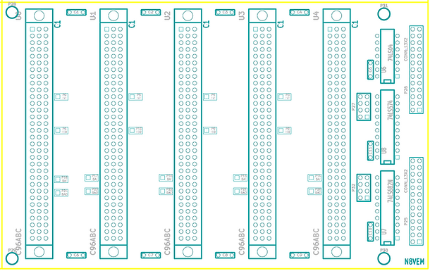
Dan Werner designed the Bridge board, which stacks up on top of the Mezzanine. Using the Mezzanine’s expansion bus, it offers five slots for normal N8VEM ECB boards. That eliminates the dependency on the Z80 host; the 6x0x becomes an expandable stand-alone computer with direct access to (for instance) the Disk IO card and its floppies/IDE drive.
The board does some small conversions necessary between the Z80 and the 6x0x world:
• The 6x0x R/W signal is not used.
Instead, OE becomes /RD and WE becomes /RD (but see Patches below)
• The separate IO space from the Z80 is mapped into 6x0x memory space
(see below under Jumpers).
• The lower address bits are tristated through the 74ls574 for IO requests [correct?].
Most signals are directly put on the ECB bus, see the table below. Left are the 6x0x signal names, right the ECB/Z80 names. Exceptions are the /MEM signal which is derived from the IO-to-memory mapping (see Jumpers below), and the MRDY signal, which is inverted into /WAIT. The M1 signal is created from E, Q, or just disabled (see Jumpers below).
Jumpers:
• P27 is a jumper block that allows the Z80’s /M1 signal to be derived from either E or Q, or just pulled
high or low.
• P32 allows the user to set a space in the 6x0x’s memory map into which ECB IO devices are mapped.
Address bits A8-A11 can be set, bits A12-A15 are hard-coded 0.
Patches and fixes:
For proper operation of the backplane, a jumper is required from PIN 10 of P25 to C22 on any one of the slots (Source: Cubix stand-alone manual). Without this, the /WR signal is not connected to the
backplane.
OS software support for the Bridge Board:
At present (August 2012), support for using the Bridge board exists for the following:
• DOS/65: The original Disk I/O card (not the V3)
• CUBIX: The original Disk I/O (not the V3) card and the VDU are supported.
The VDU requires a 2Mhz 6809 and the VDU will need a small modification, though.
It adds monochrome video, VT-52, PS2 Mouse and Keyboard, and Centronics Parallel to
the system. Only DD, not HD disk formats are supported by the disk IO card under Cubix.
• FLEX 2.0: no support – the floppy disk driver proved troublesome

Appendix 1: 6x0x Processor board details
Jumper settings for operating only the Processor board, in Host mode: (Source: Dan Werner)

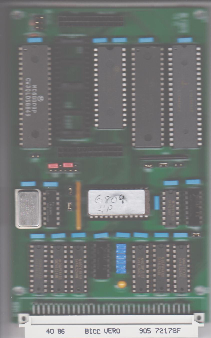
Pictures of board setup for various CPUs: (Source: Dan Werner)


Appendix 2: Mezzanine board details
Building the board should be straightforward but understanding the configuration latch and the RAM/ROM intercepts is important. Recommendation from Andrew Lynch is to
“build the 6809 IO mezzanine without U11 at first and see if you can get the ACIA, PTM, and VIAs to work as plain IO expansion. Then try to get the A16 logic working and then” [if you are planning to use the Bridge board] ”connect the expansion RAM/ROM chip select circuitry”.The 6809 IO mezzanine RAM/ROM circuitry for the expansion bus is not very useful unless the Bridge board is used.
Picture of the IO Mezzanine board set up, source Nik Brizevac (here):

Appendix 3: Operating System Software
[Forthcoming]


