Obsolescence Guaranteed
Recommended: Gigatron
a computer w/o a microprocessor

The N8VEM: Technical Design
This article describes the technical design of the N8VEM Single-Board Computer. It does not cover any expansion options available through the ECB bus or mini-IDE board. After a short overview, the logic design of each functional block is described in separate sections.
N8VEM Overview
The N8VEM board contains the minimal components needed to run a CP/M system: 512K static RAM memory, which also provides a RAM disk for storage; 1024K of ROM, containing the operating system and a large ROM disk ; a 16550 serial interface IC; and a 8255 parallel interface. The RAM can be battery powered to convert it into non-volatile storage using a DS 1210 power controller and the battery can also drive a DS 1302 real-time clock.
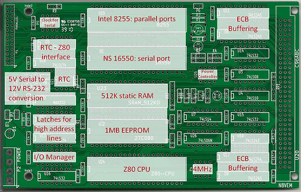
The rest of the on-board electronics glues these ICs to the Z80 and adds support for expansion cards on the ECB bus. The main functional blocks are shown on the above illustration; the chips that are not marked are simple supporting logic gates that play a role in more than one functional block.
Thanks to the small chip count, understanding the N8VEM itself is quite easy, and builders can add functionality like graphics subsystems or floppy disks afterwards.

The $20 N8VEM Single-Board Computer

1. Basics of operating the Z80 microprocessor
Section 1 is provided only for readers who are new to homebrewing. It offers a minimum of background knowledge to understand what follows in the rest of this document. If you have even a basic understanding of digital electronics you can safely skip this section.
The Z80 CPU is an attractive starting point for homebrewers. It is actually the simplest processor to get up and running. Essentially, the Z80 needs a clock signal and a one-off reset signal to start up. After a reset, it simply begins executing instructions from the first byte (address $0000) in memory, driven on by the rhythm of the clock signal. It writes and listens to the outside world using three buses, three groups of signal lines that control its interactions with the rest of the computer.
The Z80 uses the 16 lines of its address bus to announce which memory address it wants to access: it outputs high (5V) and low (0V) voltages on the bus to create the binary address of the particular byte in memory. So, right after reset, the address bus contains 16 low signals to form the startup address $0000. If it wants to write to that memory address, it outputs 8 bits of data on the data bus. If it wants to read from that memory address, the Z80 samples the data bus on the assumption that some other chip has put the value of that memory byte on the 8 data lines. Lastly, a control bus contains various signals that help to keep an orderly flow and timing on the data bus. One of the signals, for instance, is /WR: this signal is set low to indicate that the Z80 wishes to write the value on the data bus into the memory chip. Another signal is the /IOREQ pin. It signals that the Z80 does not wish to address a byte in memory, but wishes to exchange a byte with an I/O device instead. I/O devices are addressed using only the first 8 lines of the address bus, so there can be no more than 256 of them.
The three buses are a given to the computer designer. Through the eyes of the Z80, the world simply consists of 65,535 memory addresses and 256 I/O addresses, of which the content is put on the data bus when it points to them by means of the address bus. Somehow, there needs to be an electronic mechanism (the address decode logic) that decides which support chips will be made to respond to Z80 calls to particular addresses. This is the core design element for any computer: the support chips on the N8VEM board need to be told which one of them should take to the data bus if the Z80 puts a particular address on the adress bus. Support chips are not very intelligent about this, they generally only have a ‘Chip Select’ or ‘Chip Enable’ pin on them that tells them to take to the data bus and act.
Chip select logic begins with only a few signals from the Z80’s IC pins. The end result must be an individual ‘Chip Enable’ signal to each of the four ICs. Input from the Z80 consists of these signals:
• /WR(ite) & /R(ea)D: pins 22 and 21 on the Z80.
If the Z80 wants to write a byte on the data bus it sets /WR low, if it wants to read off the data bus, /RD is set low.
• /MREQ(uest) & /IOREQ(uest): pins 19 and 20 on the Z80.
If the Z80 wishes a memory chip to do something on the data bus, /MREQ is set low.
If the Z80 wants to communicate with other chips, I/O devices, then /IOREQ is set low.
Combining these four pins exactly defines whether the Z80 wants to read or write, and whether it wants to do that to a memory location (the one set on its address bus, of course) or to the port of some I/O chip (in which case the first 8 bits of the address bus should be interpreted by an I/O device rather than a memory chip).
Example from a software perspective:
Suppose the first two bytes in memory are $D3 and $FF. After a reset, the Z80 puts address 0000000000000000 on the address bus, and sets /MREQ and /RD low for a moment. The memory chip is triggered to respond to those signals by putting 11010011 ($D3) on the data bus. The Z80 reads the data bus, and executes its internal instruction number $D3, which happens to be the OUT instruction. The Z80 now puts 0000000000000001 on the adress bus, puts /MREQ and /RD low again, and gets the byte $FF from the data bus. Now it knows the complete instruction: OUTput the value in its internal accumulator (whatever that number is, that’s not defined here) to I/O address $FF.
So, it puts $FF (11111111) on the address bus (remember, I/O addresses are 8 bits long only!), puts whatever value is in the accumulator on the data bus and sets /IOREQ and /WR low for a moment. Whatever I/O chip is triggered by address $FF and the /IOREQ signal needs to pick up the value on the data bus ‘and do something with it’.
Actually, as we’ll see later, this is not the entire truth due to another circuit. The Z80 always sees the same physical bit of RAM in its upper 32K. But ignore this point for the moment.
If a Z80 is only hooked up to a single ROM and a single I/O chip, the above would be sufficient. Each of those chips will have (a) a Chip Enable pin that can be connected to /MREQ or /IOREQ, and (b) Read/Write pins to hook up to /WR or /RD. But in reality, there are three complicating factors that need to be solved by putting address decoding logic in-between:
a. There is more than one memory chip, and more than one I/O chip.
Which one should respond to a particular address?
b. Memory chips have more storage capacity than the Z80’s 16-bit address bus can address.
It means that memory chips have more data lines, how to drive them if the Z80 cannot do it directly?
c. Although the computer has to start off with ROM memory at address $0000 when it is switched on
(it needs to run something, and RAM is empty at that point), later on the ROM is no longer necessary and
should be ‘switched out’ to make place for RAM memory in its place.
Address decoding logic is built up from very simple components packed in 74LSXX chips. For instance, the 74LS08 ‘AND gate’ contains two input pins. If-and-only if both are high (5V), its output pin becomes high. The 74LSXX chips on the N8VEM schematic are easily Googled to find out what logic functions they provide. One last thing to keep in mind: the signals from the control bus are inverted. So /WR goes low (binary 0, not binary 1) to signify that the Z80 wants to write to the data bus. This is true for all signals whose name starts with a slash.
The above is only a crude summary of CPU operations, with some important omissions and simplifications. But it will enable you to understand how the N8VEM is wired up from the following sections.
2. Connecting RAM and ROM
ROM is connected to the data bus and address bus lines A0..A14. Address line A15 is actually routed separately through the memory manager logic described further down. The reason is that the upper half of the N8VEM’s memory space always contains the same RAM (‘no matter what’, to protect the CP/M OS that runs in it). Having A15 under software control ensures that any 32K chunk of ROM (either the bottom 32K of a 64K page, or the top 32K of a 64K page) can be switched into the bottom 32K page. Not having A15 under software control would waste half the ROM capacity as inaccessible.
The ROM, having more than the maximum 64K that the Z80 can address, uses more than the Z80’s 16 address lines. A16..A19 address lines (similar to A15) are under software control via the memory manager described later on. Note that jumpers K1, K6 and K8 allow smaller EPROMs to be used if desired.
RAM is connected in the same way. Jumper K7 allows a smaller 128K RAM to be used if desired. One thing of note is the battery-backup circuitry that can power RAM memory when the N8VEM is switched off. A DS1210 IC is used to sense the normal power supply. If voltage falls below the minimum threshold, the DS1210 powers the RAM from its battery instead. At the same time, the RAM Chip Select signal that goes into the DS1210 is no longer sent through to RAM, and RAM thus becomes non-responsive and falls asleep to minimise power consumption.
The Chip Select lines are input for the RAM and ROM chips – they are N8VEM’s means to get them to respond to the data bus: if the RAM Chip Select signal goes low, either the memory chip copies the data bus into its memory, or outputs the requested data byte onto the data bus. The generation of the right Chip Select signals for the right ICs is the topic of the next section.
3. The N8VEM address decoding logic
Introduction
The N8VEM has a circuit that acts as its I/O Manager. On behalf of the Z80, it controls the two obvious I/O devices: the serial interface and parallel interfaces. But in addition, there’s also a Real-Time Clock which is accessed as an I/O device. And the RAM/ROM chips are managed by a fourth I/O device, which you could call the N8VEM Memory Manager. The Memory Manager determines which chunks of on-board memory are accessible on the Z80 data bus. It switches chunks of memory in and out of view of the Z80. Before we go into a description of the Memory Manager we should first look at how the I/O management is constructed out of a set of simple 74LSXX logic ICs. Its purpose is to generate separate Chip Select lines for each of the four I/O devices mentioned, so that the right one is woken up to the data bus, given a specific address request from the Z80.
A. I/O Manager: address decode logic
A 74LS10 3-input NAND and two 74LS32 OR gates are used to generate the main /IOSEL signal. In short, if address lines A5, A6 are high, A7 and /IOREQ are low, then the N8VEM assumes that the Z80 CPU wants to select one of its four on-board I/O devices. From a programming perspective: all I/O requests to ports $60-$78 are reserved for on-board devices, any other port can be used by external ACB cards.
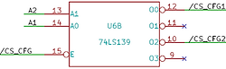
Which I/O device? That depends on the value of address lines A3 and A4. A 74LS139 decoder IC is triggered by the /IOSEL signal to sample A3 and A4 on the data bus, and use their values to determine which of the four IO devices is to be activated. 00 means that the 8255 is enabled, 10 means the 16550 serial port, 01 is the real-time clock, and 11 wakes up the Memory Manager.
The relevant part of the N8VEM schematics is shown below:
This logic also means that any ECB expansion card should be configured not to use the I/O addresses 96-127. They are reserved for the four on-board I/O devices. We can also now derive the exact I/O addresses reserved for each of the four on-board devices: A3=1 and A4=0 means the 16550 UART serial device. A5, A6 and A7 need to be 110. That leaves address lines A0-A2 as undefined by the logic schema above, creating a range of I/O adresses reserved for the 16550 between binary addresses 00010110 ($68 hex) and 11110110 (119 decimal/$6F hex).
Before we go into the memory manager itself, we should note
that the /CS_CFG signal generated above is to be split into
separate signals for configuring addressing logic for RAM and
ROM. The LS139 implements this electronically.
In words: if the combination of A1 and A2 contains the value
00, then /CS_CFG1 goes low (aimed at configuring RAM, see
further below) else, if it contains the value 10, /CS_CFG2
goes low (aimed at the ROM)
B. The memory manager
The RAM and ROM chips are larger than 64K each, meaning that the 16 address lines of the Z80 are insufficient to form a complete address for every byte in the chips. The chips have more address lines than the Z80 does. The N8VEM solves this by connecting the higher address lines of the two memory chips to two 74LS174 chips. This means that the LS174, every time its Chip Select (CP, pin 9) is driven low for a moment, takes a snapshot of the data bus lines and keeps outputting their values for use as the upper address lines.
So – the N8VEM needs two Chip Select signals (called /CS_CFG1 and CS_CFG2) as input for the two 74LS174s, each of them driving the upper address lines of the RAM and ROM memory chips respectively. Whatever bit pattern was on the data bus, then becomes the bit pattern for the adress lines above the 16 that are taken care of by the Z80 itself. For the ROM, these extra address lines are called A15..19ROM and they go straight into the ROM chip. For RAM, they are called CFG1_Q0..3, and they get some further treatment described below. Note that the LS174 which is used for the RAM addressing also contains a special signal called /ROM_ENABLE, to be discussed further below. And lastly, note that the reset signal will make all these address lines go to zero, to create a nice predefined situation at startup.
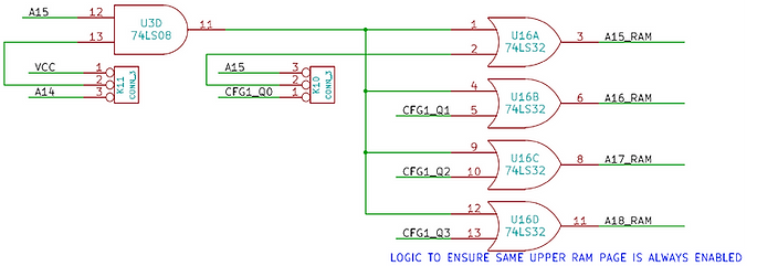
The above is the core of the memory addressing logic in the N8VEM, but there is a further step for the RAM, as shown in the figure below. This logic serves to protect the CP/M operating system by freezing the same physical RAM memory in place for the upper memory, no matter what. Setting jumpers K10 and 11 to their default (connect 1-2 for both) means this applies to the top 32K. The logic then reads as follows: “if A15=1 then force A15…18_RAM to 1 no matter what the CFG1_Q0..3 lines tell you”. The reason for this is that the CP/M operating system resides in the upper half of memory. If you switch the address lines to make another piece of RAM appear here, the OS could crash spectacularly. So, in essence, the N8VEM allows the programmer to switch the higher address lines for memory visible in the lower 32K of the Z80’s memory space, but it’s always the same (RAM) memory you’ll encounter in the upper 32K.

Example from a software perspective:
The address 00011110 ($78) activates /CF_CFG1 for RAM; 00111110 ($7C) activates /CF_CFG2 for ROM. The ROM code is quickly explained by the figure below:
The instructions LD A,00 --- OUT ($78),A --- OUT ($7C),A would clear all the output lines of both LS174s. All upper address lines would be set to 0, meaning the Z80 sees the lowest 64K in its memory chips (see sideline). In addition, the /ROM_ENABLE line is set to 0, meaning (see next section) that any access of the Z80 to the bottom 32K of its memory map is routed to ROM. The instructions LD A, $FF --- OUT ($78),A --- OUT ($7C),A would switch all lines to high, meaning the Z80 now sees the highest 64K of its memory chips. In addition, the ROM is switched out for RAM from the Z80’s view.


4. The reset and boot mechanism
Only one further mechanism needs to be set up. After reset, the N8VEM needs to find ROM at the bottom of its memory map. Later on, that ROM can be switched out and be replaced by RAM for a nice, clean 64K RAM memory space. The schematic below takes the signal /ROM_ENABLE from the RAM memory manager (it is one of the outputs in the LS174 that also takes care of the higher address bus lines, see the schematic under Memory Manager). This means that the user can set this signal to high – but that after a reset, the LS174 always sets it to low. The figure below shows how a low /ROM_ENABLE and a low A15 forces a Z80 memory request to lower memory into the ROM Chip Select – and in any other case, into the RAM Chip Select.
The power-on circuit of computers is always a compromise between robustness and simplicity. After switching on, you want the power source to be stable before starting the computer. More crucially still, if the user presses the reset button, that will not necessarily lead to a clear on/off signal. Measured in nanoseconds, the button will bounce a few times and make an ugly transition between high and low voltages. N8VEM takes a pragmatic approach to these problems: the circuit buffers the button a bit with capacitors and resistors – and then feeds it into and 74LS14 inverter. The inverter is left with the task of providing a clean high/low signal from what may be a slightly messy low/high signal going into its input ports. Routing that signal through a second inverter brings back the clean /RESET signal used across the N8VEM board. P6, by the way, provides a connector for an external reset button next to the one on the board.


5. The ECB bus
The ECB bus is, in principle, nothing more than a connector offering the data, address and control bus of the CPU to the outside world. To protect the on-board electronics from any spikes or excessive loads, though, the ECB bus is fully buffered. That means that all the lines are fed through 74LSXX chips that are supposed to take the load of sending signals through to the ECB bus, and take the hit of any inbound signals that are somehow not perfect.

For one-way signals on the control bus, a simple 74LS244 is enough. It takes in the signal on its input pins, then sends it through on its output pins.
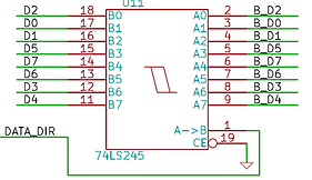
But for the data bus, where data flows in two directions, a 74LS245 is needed. Pin 1 of the LS245 is connected to the DATA_DIR signal. If DATA_DIR is low, the data bus is ‘exported to’ the ECB bus, and if it is high, the data bus signals from the ECB bus are imported from the ECB bus for reading by the Z80.

Note that the address bus too, is buffered by a two-way LS245. Although normally, the address bus is only driven by the Z80 CPU, peripherals can send a /BUSRQ signal to the Z80 to request control of the address lines. The Z80 will signal its approval by sending /BUSAK low and decouple itself from the address bus. This is why /BUSAK is also the switch to the LS245 buffering the ECB bus: it will allow address bus signals to come in from the ECB bus only if the Z80 approves it. Now, a peripheral on the ACB bus could take over and perform DMA (Direct Memory Access) whilst the Z80 is decoupled.
Whereas the address bus has two-way traffic only in exceptional circumstances (DMA peripherals), the data bus sees constant two-way traffic. The LS245 buffering the ECB bus is switched to accommodate traffic from either direction through the DATA_DIR line, which is created by the logic below:

Interpretation of the circuit driving the data direction of the LS245 data bus buffer chip:
Part 1 (top left) – The LS08 AND gate evaluates whether this is a request to an on-board device (i.e., any memory request or an IO request where the I/O decode logic recognises one of the four on-board I/O devices), in which case the LS08 output goes low. Otherwise, the LS08 output goes high to signify an off-board ECB bus request. Combined with the /RD signal through the LS32 OR gate, the result is a high signal if and only if this is an I/O write request from the Z80 that is not addressed to an on-board chip.
Part 2 (bottom left) – First, a Z80-specific fact: if the Z80 signals an /IOREQ, then /M1 going low signifies the Z80 is acknowledging an interrupt and wishes to read the interrupt data from the data bus. Part 1 already screens for an (off-board) /IOREQ. So, with that background knowledge, Part 2 becomes clear: The LS10 NAND gate starts to output a high signal in one of three cases: if (/RD:) the Z80 wishes to read something, or (/M1:) if the Z80’s M1 timing signal could mean the desire to read the bus due to an interrupt acknowledge, or (/BUSAK:) is in a phase where the Z80 has disconnected itself from the data to allow DMA.
Part 3 brings the two components together on an LS08 AND gate: the signal line DATA_DIR that goes to the ECB buffer chip is high only when the Z80 wishes to read something from an off-board device.
One thing should be noted explicitly: the above circuitry means that the N8VEM can use the ECB bus only for I/O devices. Memory is hard-wired to be only the on-board RAM and ROM. In practice, this may not be such an important limitation as there is rather a lot of memory on-board, but still – it is a hardware constraint.
6. Connecting the 16550 UART
The I/O address decoding logic drives the /CS_UART Chip Select signal, which tells the 16550 to become active on the data bus. In the section on the N8VEM’s IO address decode logic, we established that activating any on-board IO device requires A5 and A6 to be high, A7 to be 0. In addition, activating /CS_UART specifially requires A3=1 and A4=0.
That leaves address lines A0-A2 undefined by the logic schema above – which comes in handy as the 16550 itself has three address lines (A0..2) that can now be connected directly to the address bus. The figure below illustrates how I/O address 01 on the 16550 can be accessed by the Z80:
As the hex equivalent of the binary number 10010110 is $69, the Z80 instruction in A,($69) reads the value of the 16550’s second register (register 01, that is) into the Z80’s accumulator. The 16550 data sheet describes the functionality of its registers.
Other than this, there is little to do to get the serial port integrated into the N8VEM system. The 16550 uses a separate clock signal for its internal baud rate generator, and a MAX 232 chip translates its output (the serial port) from 0V/5V signals into -12/+12V signals as required by the RS-232 standard.
Also, the 16550 can generate interrupts, and these are fed into the Z80’s /INT line through a LS06 inverter (because the 16550 sends a high interrupt signal whilst the Z80 needs a low interrupt signal). After that, a strange thing happens: the 16550’s interrupt signal is led to the /INT pin on the ECB bus, from where it is brought back into the N8VEM board through two more inverters. This is, er, for hysterical raisins...
7. 8255 parallel I/O
The 8255 is perhaps the most well-know parallel IO chip of its era, providing three 8-bit I/O ports. It is simply connected to the data bus, and its address lines A0 and A1 are connected on the address bus to make its internal registers accessible to the Z80 as I/O ports. The /CS_PPI line acts as its Chip Select signal. It cannot generate interrupts. Lastly, see the last section of this text for a crucial configuration setting governing the parallel port connector.
8. The Real-Time Clock
A standard DS1302 is used to keep the time. It is attached to a 32Khz crystal and fed with battery power to keep it going. It needs to be accessed by the Z80, both for reading the time and setting it. Battery power may be attached directly to a 2-pin connector on the board, or it may be obtained from the 96-pin ECB connector, if the backplane provides battery power.
As opposed to the other I/O chips, the DS1302 does not have a separate Chip Select signal. Instead, two LS32 OR gates are used to blend the Z80 /RD and /WR signals together with the /CS_RTC coming from the IO address decoder logic, resulting in /RTC_RD and /RTC_WR signals.
This chip does not communicate straight onto the data bus either. It does input and output on a single pin in a serial fashion. The LS174 buffers all inputs to the DS1302 input pins, and on D5/BUF_Q5 controls the direction of data flow into or out of the clock chip. After a Reset signal (RST) is applied through the LS174 to the clock chip, a command byte is clocked into the DQ input by toggling the Clock (BUF_Q6) and Data (BUF_Q7) bits. The command is either a read or write. If it is a write, date / time or clock control information is toggled into the chip in a fashion similar to writing the command byte. If the command is a read, then BUF_Q5 is deasserted to read back the data output from the clock chip on D7. The data is output one bit at a time, one bit for each clock pulse, in a serial fashion. The use of the LS174 in this fashion is referred to as "bit-banging", since each signal transition is controlled by an /RTC_WR of a data byte to the LS174. Each bit input, is read on D7, under control of the output that enables the LS125 from BUF_Q5.


9. Summary
Z80-based computers can be surprisingly simple, as long as complicating factors such as floppy disks or video circuitry are kept off the main board. As the N8VEM shows, even a flexible memory manager can be implemented with only a few logic gates and a latch. The real-time clock circuitry is actually the most complex part of the N8VEM board – but is only of secondary importance.
Appendix: Differences between N8VEM Mk. 1 and 2
The above article describes the Mk. 2 SBC. The differences between the first and second release of the N8VEM board are small, and summarised below:
• The Mk.1 board ignored the CTS/RTS lines on the serial port. Hardware handshaking was done with the DTR/DSR lines instead, which is unusual.
The Mk.2 has on-board jumpers (K2-K5) that allows the user to select which ones are driven by the MAX-232 and brought out on the serial connector.
• The Mk.2 board adds the DS1210 battery-backup capability. Mk.1 users sometimes used a battery-backed SRAM for the same purpose,
but that was a rather costly option.
• Instead of the simple power led on the Mk.1, the Mk.2 has a bicolor led that shows power-on as well as the /HALT line.
Which can be of use as a debigging instrument.
• The Mk.1 parallel port (connected to the 8255) has GND signals on pins 25 and 26.
Via jumper K9, Mk.2 boards can supply +5V power through pin 25 – but clearly that makes the Mk.2 lethally incompatible with the Mk.1 parallel port!
Mk.1 users are recommended to cut the trace leading up to pin 25 for that reason.
• The Mk.1 board did not export the Z80 clock signal to the ECB bus, with the idea that this would not really be needed by peripheral boards and would
only lead to interference on the backplane. However, some boards do need the clock signal and the Mk.2 duly brings it out onto the ECB bus.
Mk.1 users are recommended to make a small patch to do the same.


